A crash course on JFETs
JFETs typically have very low current noise and this property makes them a great option for low noise amplifiers. Before we go into the details of the design, let take a quick look at the physics of the device.
The geometry
The junction field effect transistor is a three terminal device as illustrated in Fig. 1. The current between two of the terminals, named as source and drain, flows through called the “channel” which may be made of either a P-type or an N-type. The third terminal, called the gate, is used to apply a voltage across the channel to control the amount of current flow.
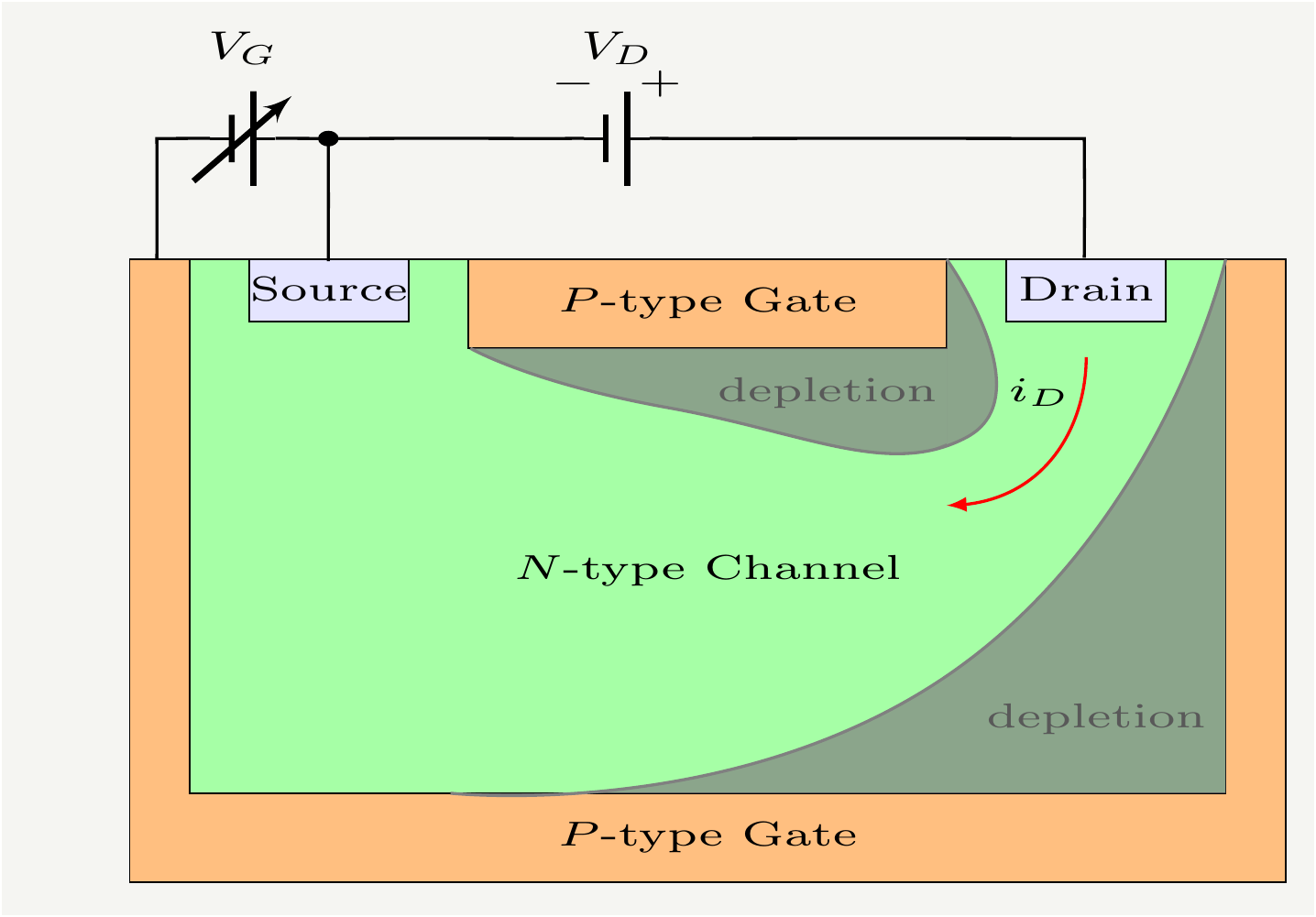
Figure 1: Operation of the jFET under reverse gate bias. Note that the gate terminals are connected internally. As the gate bias gets more negative, the depletion regions will pinch the channel completely. In that case the drain-source current will be fixed and independent of the drain source voltage.
jFETs are unipolar devices, in which the current is carried by only one type of carriers, electrons or holes depending on the channel type, not both at the same time. This is in contrast with bipolar transistors that make use of both holes and electrons at the same time to conduct current. The Field Effect Transistor gate current is much smaller compared to bipolar transistors, and therefore they have a much larger input impedance. Since drain current is controlled by the gate voltage, jFETs can be modeled as a voltage controlled current source. Figure 2 shows the circuit symbol for N and P channel jFETs.

Figure 2: Circuit symbols for N and P channel jFETs.
I-V curves
The Gate-Drain junction of the jFET is under reverse-bias. This creates the depletion region that is free of charge carriers. The size of the depletion region will increase as \(V_{G}\) becomes more negative reducing the drain current. Similarly, after the "pinching point’’, for large enough \(V_{DS}\), further increasing \(V_{DS}\) will not increase the drain current since the device is now in the saturation mode. This is because the additional voltage will be dropped across the depletion region. The I-V characteristics of the device is shown in Fig. 3.
](jfetregions.png)
Figure 3: I–V characteristics and output plot of an n-channel JFET . Credit:Wikipedia
The most important curve is the one on the right hand side of the Fig. 3 which shows the drain current in the saturation region for a given value of the gate voltage. That curve is quadratic in nature, which we will derive later, and is approximately given by \[\begin{eqnarray} I_D=I_{DSS}\left(1 - \frac{V_{G}}{V_P} \right)^2\tag{1}, \end{eqnarray}\] where \(V_P\) is the pinch-off voltage and \(I_{DSS}\) is the current at \(V_{G}=0\).
The derivation of Eq. (1) is a bit involved, but we can at least provide a sketch of it. The first thing we will need the depth of the depletion layer, and that can be computed as in the standard p-n junction analysis. When p and n type semi-conductor meet at an interface, electrons and holes will move across the interface and the p type material will build up excess negative charges and the n type material will build positive charges, as shown in Fig. 4
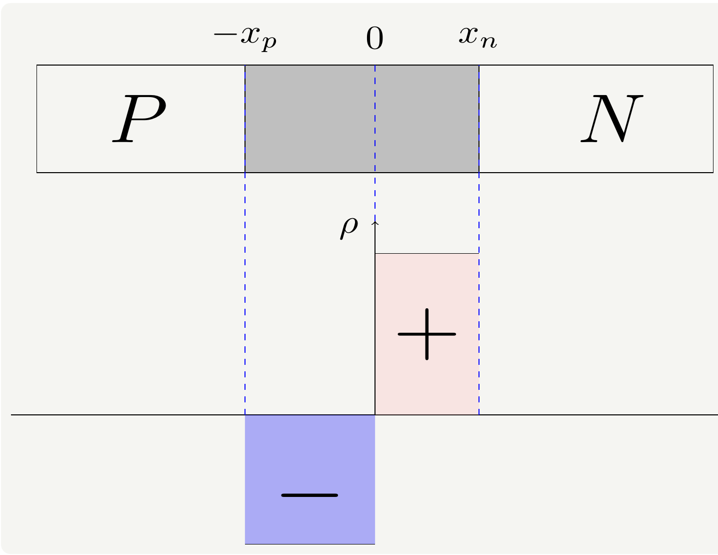
Figure 4: A depletion region forms around the interface of p and n type semiconductors. On the top is the geometry of the device, on the bottom is the charge density.
Given the charges around the interface, we can calculate the electric field using the Gauss’ law \[\begin{eqnarray} \mathbf{\nabla}\cdot\mathbf{E} &=& \frac{\rho}{\varepsilon_s}\, \implies \, \frac{dE}{dx}=-\frac{q N_A}{\varepsilon_s}, \tag{2} \end{eqnarray}\] where we made use of the fact that there is electric field only along the \(x\) axis. This equation applies to the region \(-x_p\leq x \leq 0\) and \(q\) is the charge of an electron and \(N_A\) is the acceptor number density. We can solve for the electric field by simple integration: \[\begin{eqnarray} E(x)=-\frac{q N_A}{\varepsilon_s}(x+x_p),\,\, -x_p\leq x \leq 0. \tag{3} \end{eqnarray}\] Same differential equation applies to the region on the right hand side: \(0\leq x \leq x_n\), and the solution is: \[\begin{eqnarray} E(x)=-\frac{q N_D}{\varepsilon_s}(x_n-x),\,\, 0\leq x \leq x_n \tag{4}, \end{eqnarray}\] where \(N_D\) is the donor number density. The electric field as to be continuous at the interface \(x=0\), and enforcing the continuity relates \(x_p\) to \(x_n\): \[\begin{eqnarray} N_A x_p=N_D x_n\tag{5}. \end{eqnarray}\] We can integrate one more time to get the potential difference: \[\begin{eqnarray} V(x)=\frac{q N_A}{2 \varepsilon_s}(x+x_p)^2,\,\, -x_p\leq x \leq 0, \tag{6} \end{eqnarray}\] where we dropped the integration constant by defining \(V(-x_p)=0\) as the reference voltage. Let’s repeat for the right side: \[\begin{eqnarray} V(x)=V_{bi}-\frac{q N_D}{2 \varepsilon_s}(x_n-x)^2,\,\, -x_p\leq x \leq 0, \tag{7} \end{eqnarray}\] where we introduced the integration constant \(V_{bi}\) since we had already declared the reference voltage point. \(V_{bi}\) is the built in voltage between the points \(-x_p\) and \(x_n\), and it is about \(0.2V\) for Ge and \(0.8V\) for Si based semiconductors. We now impose the continuity of the voltage across the interface by setting Eqs. (6) and (7) equal to each other at \(x=0\), to get: \[\begin{eqnarray} V_{bi}-\frac{q N_D}{2\varepsilon_s}(x_n)^2= \frac{q N_A}{2 \varepsilon_s}(x_p)^2 \tag{8} \end{eqnarray}\] We can make use of Eqs. (5) to solve for \(x_n\) and \(x_p\) and add them up to get the total depletion width:
\[\begin{eqnarray} x_n&=& \sqrt{\frac{2 V_{bi}\varepsilon_s}{q} \frac{N_A}{N_D(N_A+N_D)} }\nonumber\\ x_p&=& \sqrt{\frac{2 V_{bi}\varepsilon_s}{q} \frac{N_D}{N_A(N_A+N_D)} }\nonumber\\ D&=&x_n+x_p= \sqrt{\frac{2 V_{bi}\varepsilon_s}{q} \left( \frac{1}{N_D}+ \frac{1}{N_A} \right) }.\tag{9} \end{eqnarray}\] The most important observation here is that the width of the depletion is proportional to \(\sqrt{V_{bi}}\). Note that this derivation assumed there is no externally applied voltage across the diode terminals. When there is a reverse bias applied, we need to add that to \(V_{bi}\). The gate-channel junction is just like a diode, and the depletion width will be set by the applied gate voltage.
How does the depletion length enter into the current equation? At the simplest level, it reduces the cross section of the channel. A channel of original height \(H\) will reduce to the height \(H-D\). The depletion width can be as large as the height, which will pinch off the channel. From Eq. (9), we can calculate the value of the gate voltage to pinch the channel when \(V_{DS}=0\):
\[\begin{eqnarray} D&=& \sqrt{\frac{4 (V_{bi}-V_P)\varepsilon_s}{q N_D} }=H, \, \implies \, V_P=V_{bi}-\frac{q N_D H^2}{4 \varepsilon_s q},\tag{10} \end{eqnarray}\] where we assumed \(N_D\simeq N_A\). For a typical set of input parameters, \(V_P\) is around \(-2.7V\).
We are going to relate the depletion width to the drain-source current using the drift speed of the charge carriers. The current density due to the drift is given by \[\begin{eqnarray} J&=& q \mu N_D E=-q \mu N_D \frac{dV}{dx},\tag{11}. \end{eqnarray}\] The total drain current is \[\begin{eqnarray} I_D= A J&=& - W (H- D) q \mu N_D \frac{dV}{dx}=- W H \left(1- \frac{D}{H}\right) q \mu N_D \frac{dV}{dx}\nonumber\\ &=&- W H \left(1- \sqrt{\frac{4 (V_{bi}-(V_G-V)) \varepsilon_s}{q N_D H^2} }\right) q \mu N_D \frac{dV}{dx} \nonumber\\ &=& - W H \left(1- \sqrt{\frac{ V_{bi}-(V_G-V) }{ V_{bi}-V_P } }\right) \frac{dV}{dx},\tag{12} \end{eqnarray}\] where used Eq. (10), and also defined \(\mu\) as the average mobility of the carriers. \(A\) is the cross-sectional area of the channel given by \(W\times(H-D)\) where \(W\) is the dept of the channel in the perpendicular direction. Note that \(I_D\) is a constant and therefore has no \(x\) dependence, and we can rewrite the integral in the differential form as follows: \[\begin{eqnarray} I_D dx = - W H q \mu N_D \left(1- \sqrt{\frac{ V_{bi}-(V_G-V) }{ V_{bi}-V_P } }\right) dV \tag{13}. \end{eqnarray}\] Integrating from \(0\) to \(L\) on the left, and from \(0\) to \(V(L)=V_{D}\) on the right we get: \[\begin{eqnarray} I_D &=& - \frac{W H q \mu N_D }{L} \int_0^{V_D}\left(1- \sqrt{\frac{ V_{bi}-(V_G-V) }{ V_{bi}-V_P } }\right) dV \nonumber\\ &=& g_0\left( V_D -\frac{2}{3}( V_{bi}-V_P) \left[ \left(\frac{V_D+ V_{bi}-V_G}{ V_{bi}-V_P }\right)^\frac{3}{2}-\left(\frac{ V_{bi}-V_G}{ V_{bi}-V_P }\right)^\frac{3}{2} \right] \right) ,\tag{14} \end{eqnarray}\] where \(g_0=\frac{W H q \mu N_D }{L}\) is the conductivity constant. We can approximate this complicated function in two zones. In the linear zone, \(V_D\) is relatively smaller, and we can expand Eq. (14) in powers of \(V_D\) and keep the first term:
\[\begin{eqnarray} I_D &=& g_0 V_D \left[ 1- \left(\frac{V_{bi}-V_G}{ V_{bi}-V_P }\right)^\frac{1}{2} \right] \tag{15}. \end{eqnarray}\]
On the other limit, we can see that \(I_D\) has a maximum value at \(V_{D}=V_G-V_P\), which can be shown by taking the derivative of Eq. (14) with respect to \(V_D\) and setting it to zero. In order to find the dependence on \(V_{G}\) in the saturation region, it is best to make the approximations before evaluating the integral in Eq. (14):
\[\begin{eqnarray} I_D &=& - \frac{W H q \mu N_D }{L} \int_0^{V_D}\left(1- \sqrt{\frac{ V_{bi}-(V_G-V) }{ V_{bi}-V_P } }\right) dV = -g_0 \int_0^{V_D}\left(1- \sqrt{\frac{ V_{bi} -Vp-(V_G-V_P-V) }{ V_{bi}-V_P } }\right) dV \nonumber\\ &=&-g_0 \int_0^{V_D}\left(1- \sqrt{1-\frac{ V_G-V_P-V }{ V_{bi}-V_P } }\right)dV \simeq -\frac{g_0}{V_{bi}-V_P } \int_0^{V_D}\left(V_G-V_P-V \right)dV \nonumber\\ &=&-\frac{g_0}{V_{bi}-V_P } \left(V_G-V_P-\frac{V_D}{2} \right)V_D, \tag{16} \end{eqnarray}\] where we crudely treated the fraction under the square root as a small number. For any given \(V_G\) the current saturates at \(V_{D}=V_G-V_P\). Plugging this in to Eq. (16), we have:
\[\begin{eqnarray} I_D(V_G)=I_{DSS}\left(1 - \frac{V_{G}}{V_P} \right)^2\tag{17}, \end{eqnarray}\] where we dumped everything in front into \(I_{DSS}\). This completes the sketch of the proof.
Small signal analysis
Amplifiers are typically operated in the saturation region which fixes the transconductance of the device. As a small signal is added to the circuit coupled to the gate terminal, it will change the gate voltage by a small amount: \(V_{G}\rightarrow V_G+v_G\). This will result in a change in the drain current. For a careful analysis, we are going to reserve the capital letters for the DC, bias quantities and small letters for signals. Starting from Eq. (17), we can see the effect of shifting the gate voltage:
\[\begin{eqnarray} I_D\left(V_{GS}+V_{GS}\right)&=&I_{DSS}\left(1 - \frac{V_{GS}+V_{GS}}{V_P} \right)^2\simeq I_{DSS}\left(1 - \frac{V_{GS}}{V_P} \right)^2 -\frac{2 I_{DSS}}{V_P} \left(1 - \frac{V_{G}}{V_P} \right) V_{GS} \nonumber\\ &=& I_D\left(V_{GS}\right)+g_m V_{GS} \tag{18}, \end{eqnarray}\] where \(g_m\) is the transconductance defined as \[\begin{eqnarray} g_m\equiv -\frac{2 I_{DSS}}{V_P} \left(1 - \frac{V_{G}}{V_P} \right) \tag{19}. \end{eqnarray}\] Equation (18) shows that the drain current is the sum of the bias current set by the gate bias voltage (\(V_G\)) and the part controlled by the deviations in the gate voltage (\(v_G\)). In this mode of operation, the JFET is nothing but a voltage controlled current source and it can be represented symbolically as in Fig. 5.
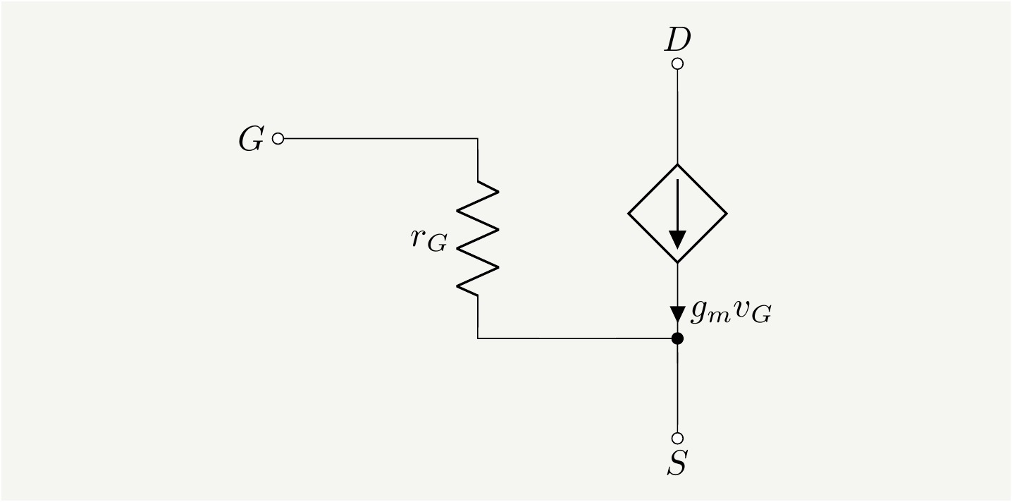
Figure 5: Small signal AC model for JFETs. \(r_{G}\) is typically very large which further simplifies the analysis.
Amplifiers
Let’s get a bit more practical and build some experience in analyzing simple amplifier circuits featuring jFETs.
Source follower
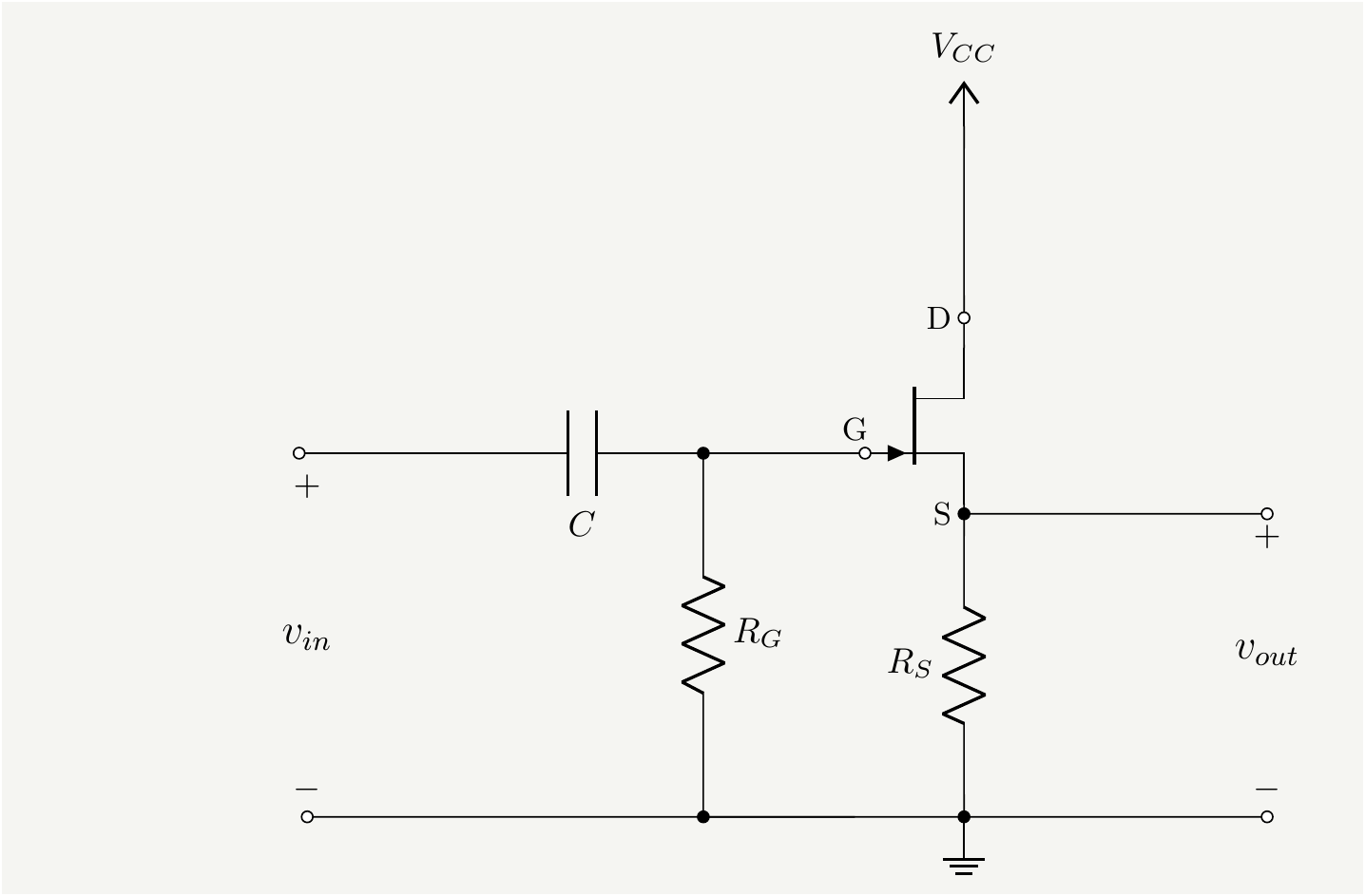
Figure 6: A simple source follower amplifier.
The operating point of the JFET is found by removing the input voltage and analyzing the I-V curve of the device. One the operating point is is calculated, the DC sources are turned off and the AC is added. Provided that the DC operating point is designed to be in the saturation region, the jFET current is then linearly related to the input signal. The superposition of sources is illustrated in Fig. 7.
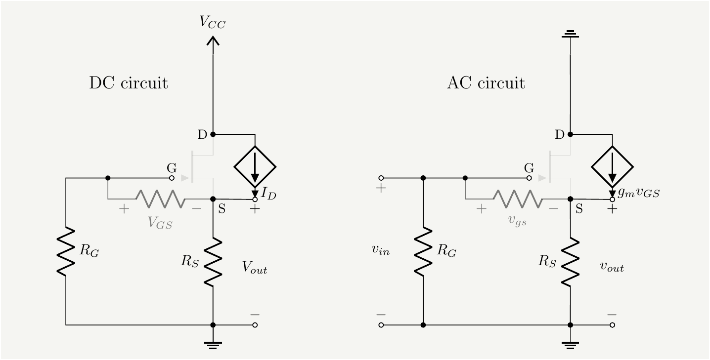
Figure 7: Left: DC equivalent circuit, right: AC equivalent circuit .
The DC circuit is as simple as it gets since the gate-source resistance, which is shown faded gray is practically infinite: there is no gate current. This tells us that \(V_{GS}=-V_S=-I_D R_S\), i.e., the gate bias is created by the drain current, which is the reason why such circuits are referred to as ``self-biased.’’ Using the formula in Eq. (17) with \(V_{GS}=-I_D R_S\) we get: \[\begin{eqnarray} I_D(V_G)&=&I_{DSS}\left(1 - \frac{V_{G}}{V_P} \right)^2=I_{DSS}\left(1 + \frac{I_D R_S }{V_P} \right)^2\tag{20}, \end{eqnarray}\] which is a quadratic equation in \(I_D\) with the following solution:
\[\begin{eqnarray} I_D&=&\frac{-2 I_{DSS} R_S +V^2_P -V_P^{3/2}\sqrt{V_P-4 I_{DSS}R_s }}{2 I_{DSS} R_s^2} \tag{21}. \end{eqnarray}\] Lets punch in some numbers: \(I_{DSS}=10\,mA\), \(V_P=-2V\), \(R_S=200\Omega\) to get \(I_D=3.8\,mA\) and \(V_{GS}=-0.76V\). We can comfortably satisfy the saturation condition, \(V_{DS}>V_G-V_P\), if \(V_{CC}>2V\).
The AC analysis is also simple. We add up the voltages in the gate loop: \[\begin{eqnarray} -v_{in} +v_{gs}+v_{out}=0=-v_{in} +v_{gs}+g_m v_{GS}R_s \implies v_{in}= v_{gs}\left( 1+g_m R_S\right) \tag{22}. \end{eqnarray}\] And the output voltage is: \[\begin{eqnarray} v_{out}=g_m v_{GS}R_s \tag{23}. \end{eqnarray}\] The gain is the ratio:
\[\begin{eqnarray} G=\frac{v_{out}}{v_{in}}=\frac{g_m R_s}{1+g_m R_s} \tag{24}. \end{eqnarray}\] For large values of \(g_m R_s\), the gain will be close to unity. What we have accomplished is taking a signal from a source which possibly had a large impedance and cloned it over to create a signal with lower impedance. In fact, we look from the load side back to the circuit, the impedance will be \(R_s//\frac{1}{g_m}\) which can be made much smaller than the impedance of the original input signal.
Common source amplifier
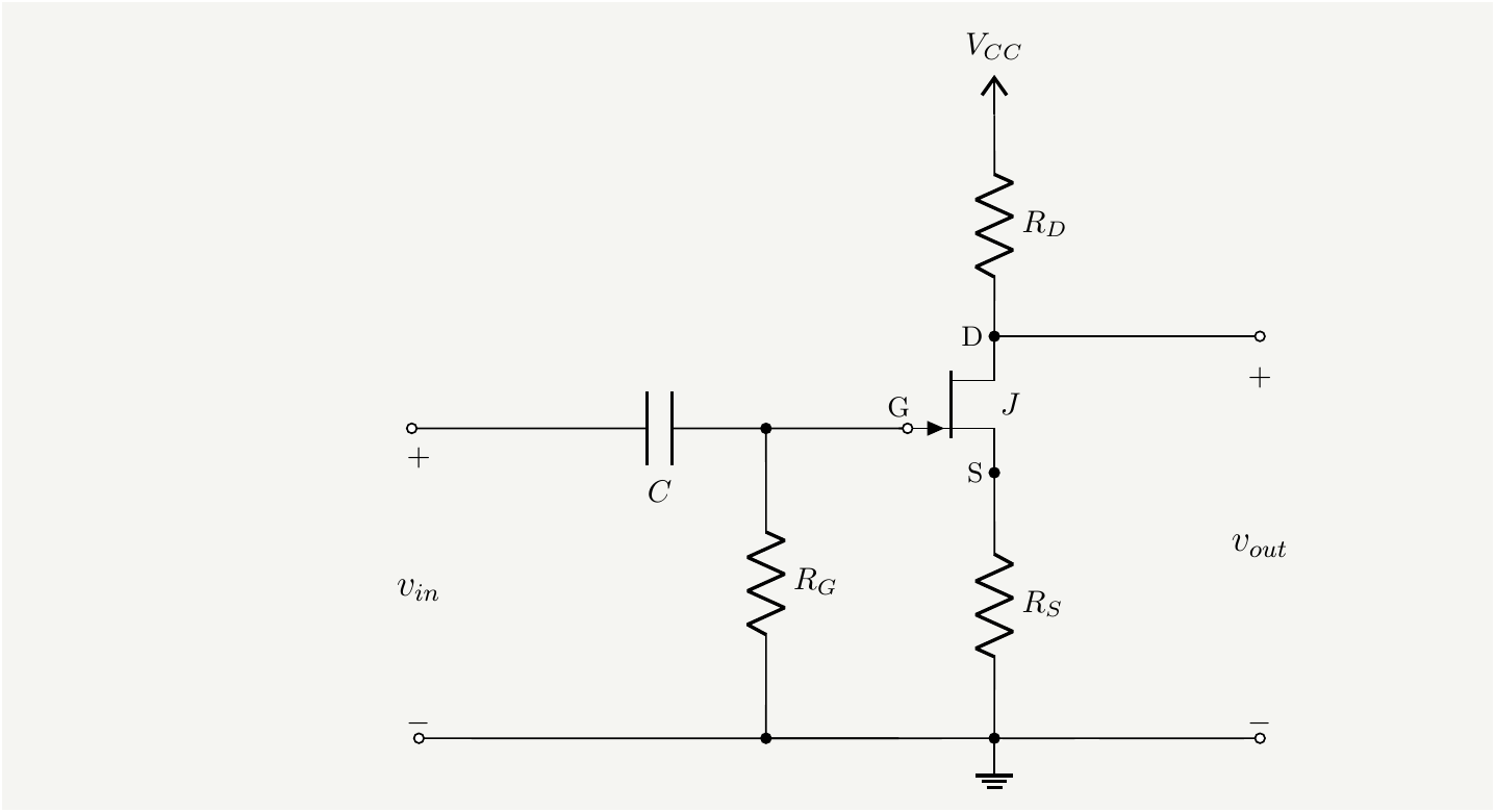
Figure 8: A simple common source amplifier.
We go through the same exercise of finding the operating point of the JFET by removing the input voltage, left panel in Fig. Fig. 9, and analyzing the I-V curve of the device. We then turn off the DC sources and add the the AC signal.
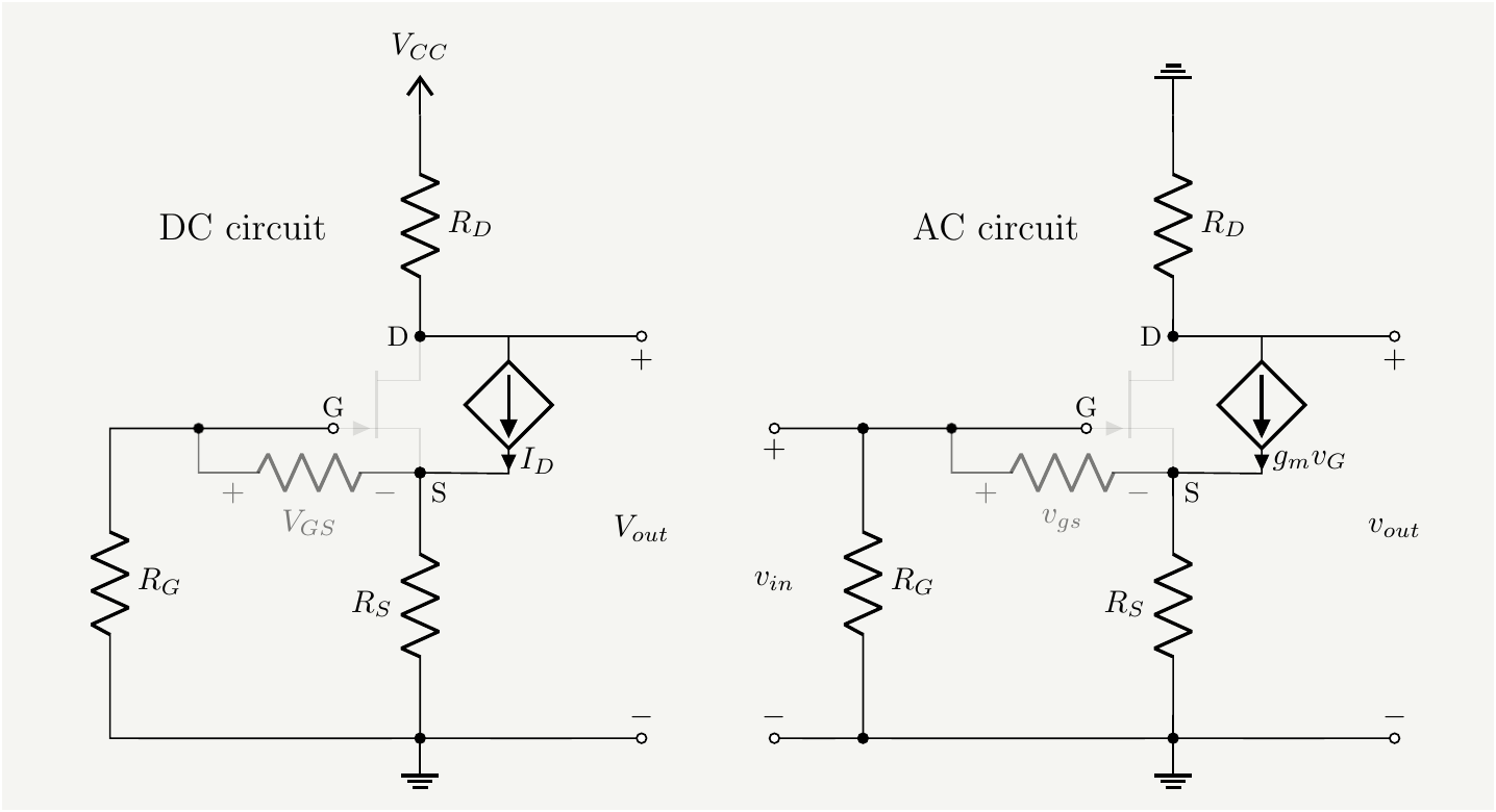
Figure 9: Common source amplifier. Left: DC equivalent circuit, right: AC equivalent circuit .
The DC analysis is identical to the source follower case. With the same input numbers: \(I_{DSS}=10\,mA\), \(V_P=-2V\), \(R_S=200\Omega\), and \(R_D=3K\Omega\), we get \(I_D=3.8\,mA\) and \(V_{GS}=-0.76V\). The voltage across \(R_D\) is \(V_{R_D}=I_D R_D=11.4V\). The power supply voltage should be such that \(V_{CC}=V_{RD}+V_{DS}\geq V_{RD}+V_{GS}-V_P\).
The AC analysis is similar to the source follower case: We add up the voltages in the gate loop: \[\begin{eqnarray} -v_{in} +v_{gs}+v_{out}=0=-v_{in} +v_{gs}+g_m v_{GS}R_s \implies v_{in}= v_{gs}\left( 1+g_m R_S\right) \tag{25}. \end{eqnarray}\] And the output voltage is: \[\begin{eqnarray} v_{out}=-g_m v_{GS}R_D \tag{26}. \end{eqnarray}\] The gain is the ratio:
\[\begin{eqnarray} G=\frac{v_{out}}{v_{in}}=-\frac{g_m R_D}{1+g_m R_s} \tag{27}. \end{eqnarray}\] Entering numerical values into Eq. (19) we get \(g_m=6.2\,mS\), and the amplification factor \(G=-8.29\).