This is the final one of a series of posts on LIGOs photodetector circuits. It builds on a few earlier posts of mine:
In this post we will look into the Advanced Laser Interferometer Gravitational-Wave Observatory (aLIGO) photodiode circuit and compute its noise performance. We then apply what we have learned in these four posts above to reoptimize the circuit and show that we can design a circuit with substantially better performance.
The model
The photodiode connects to the rest of the circuit as shown in Fig. 1.
![The photodiode connected to the notch filters, collapsed into a single impedance, and the selectors. <span class='plus'>... [+]</span> <span class='expanded-caption'> Notch filters knock out the unwanted harmonics and the frequency selectors will take in the targeted frequency while rejecting everything else.</span>](placeholder.png)
Figure 1: The photodiode connected to the notch filters, collapsed into a single impedance, and the selectors. … [+]
Although we will be dealing with a fixed number of notches and readouts in this particular problem, it will be worthwhile to build the model in a generic way so that it will be applicable to an arbitrary number of notches and readouts. As we are developing the model in the most generic sense, we will want to develop the numerical analysis code in the same way so that it can handle arbitrary circuits. Furthermore, at any point in the numerical analysis, we will want to be able to automatically create a circuit in LTspice, simulate it there and collect and analyze the resulting data. This is more complicated than simply passing parameters to LTspice since the topology of the circuit itself may change. We will need to get creative to make this work! Let us start with the mathematical model. In Fig. 1, we already collapsed the notch filters into a block and called the impedance of that block \(\vec{Z}_{N}\equiv\{Z^1_N,Z^2_N,\cdots,Z^n_N\}\), and we will also collapse all the readout filters into \(\vec{Z}_{R}\equiv\{Z^1_R,Z^2_R,\cdots,Z^m_R\}\). With these blocked elements, the total impedance is simple to write down: \[\begin{equation} Z_T=Z_d+\text{para}\left(\vec{Z}_{N},\vec{Z}_{R}\right) \tag{1}, \end{equation}\] where \(\text{para}()\) returns the parallel impedance.
The voltage at the \(i^\text{th}\) readout port is given by the simple voltage division: \[\begin{equation} V^i=I Z_{C_D} \frac{\text{para}\left(\vec{Z}_{N},\vec{Z}_{R}\right)}{Z_T} \frac{Z^i_\text{R,out} }{Z^i_R}, \tag{2} \end{equation}\] where \(Z^i_\text{R,out}\) is the impedance of the circuit element the readout voltage is measured on. It will be a capacitor in parallel with a resistor for the DC output. It may be an inductor for the other readouts.
We can define a trans-impedance which converts the input current \(I\) to \(V_\text{out}\): \[\begin{equation} Z^i_\text{tr}\equiv\frac{V^i_\text{out}}{I}=Z_{C_D} \frac{\text{para}\left(\vec{Z}_{N},\vec{Z}_{R}\right)}{Z_T} \frac{Z^i_\text{R,out} }{Z^i_R} \tag{3}. \end{equation}\]
An input current of amplitude \(I_j\) and angular frequency of \(\Omega_j\) will create a voltage at the readout port \(i\) (also the OPAMP input) as \[\begin{equation} V_j^i=I_j Z^i_\text{tr}(\Omega_j) \tag{4}. \end{equation}\]
The spectrum of the input signal from the photodiode is given in Tab. 1, and the spectrum shows very narrow spikes at multiple frequencies [1].
| name | age | gender |
|---|---|---|
We can calculate the current amplitudes \(I_j\) using the power values at various frequency in Tab. 1 and using a conversion efficiency of \(0.86\).
The thermal noise will appear at the OPAMP port. That noise is created by the real part of the equivalent impedance, which we will refer to as backwards impedance. Consider the read out port \(i\): \[\begin{eqnarray} Z^i_\text{BO}&\equiv&\text{para}\left( Z^i_\text{R,out},\text{para}\left(\vec{Z}_{N},\vec{Z}^{-i}_{R}\right)+Z^i_\text{R,in}\right)\tag{5}. \end{eqnarray}\] The notation needs some explanation:
- \(Z^i_\text{R,out}\): the filter element the read out is measured on
- \(Z^i_\text{R,in}\): the complementary element of the filter.
- \(\vec{Z}^{-i}_{R}\): the read out impedance vector excluding the \(i^\text{th}\) filter.
We can now define the pseudo SNR at readout port \(i\) as follows: \[\begin{eqnarray} \text{pSNR}^i=\left.\frac{\left|I_\text{shot} Z^i_\text{tr}\right|^2}{4k_B T \Re\{Z^i_\text{BO}\} +\left|i_\text{op} Z^i_\text{BO}\right|^2+\left(V^o_\text{v}\right)^2} \right\rvert_{\Omega_i} \tag{6}. \end{eqnarray}\] We may have \(m\) such readout ports, to which we can assign weights and define a weighted average pSNR:
\[\begin{eqnarray} \overline{\text{pSNR}}=\frac{1}{m}\sum_{i=1}^m \text{w}_i\, \text{pSNR}^i \tag{7}, \end{eqnarray}\] which is the metric we will want to maximize. We will require that the unwanted content in the spectrum to not saturate the OPAMP input:
\[\begin{equation} V^i\equiv \sum_{j\neq i} V_j^\text{i}= \sum_{j\neq i} I_j Z^i_\text{tr}(\Omega_j) < V_\text{sat}\,, \forall\, i \tag{8}, \end{equation}\] where the summation is done for all terms in the spectrum except for the targeted readout frequency, i.e., only the cross terms are added up. With Eqs. (7) and (8) the mathematical formalism to optimize the circuit is completed. We can now turn to building the numerical analysis machinery for the computation.
The code
In order to pass the circuit created in the optimization loop to LTspice in automated way, we create a set of building block templates in LTspice, as shown in Fig. 2. These blocks are completely defined by their input and output terminals and the place holder values for the elements.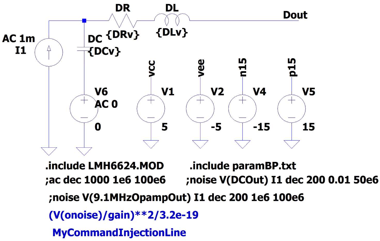
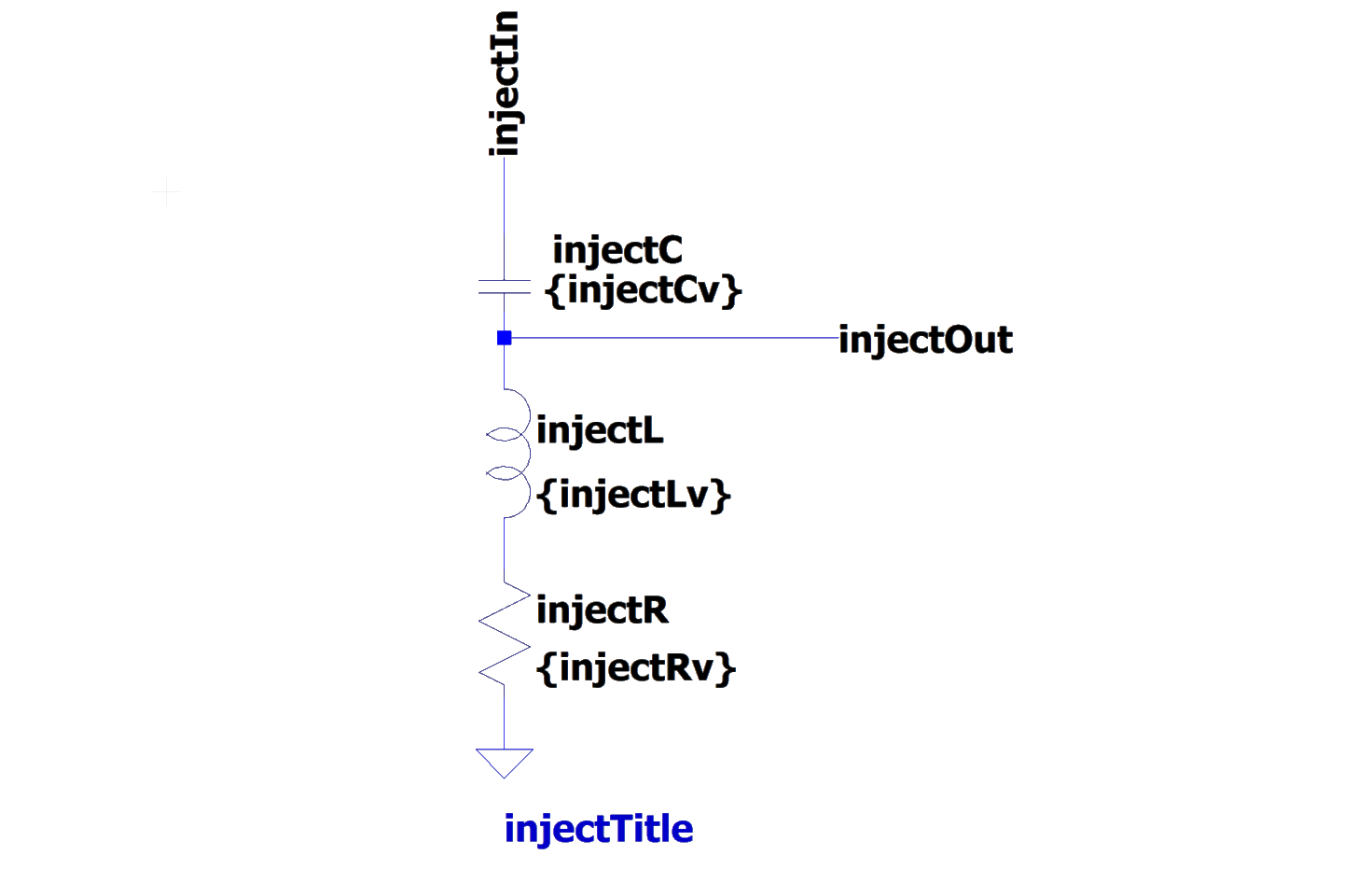
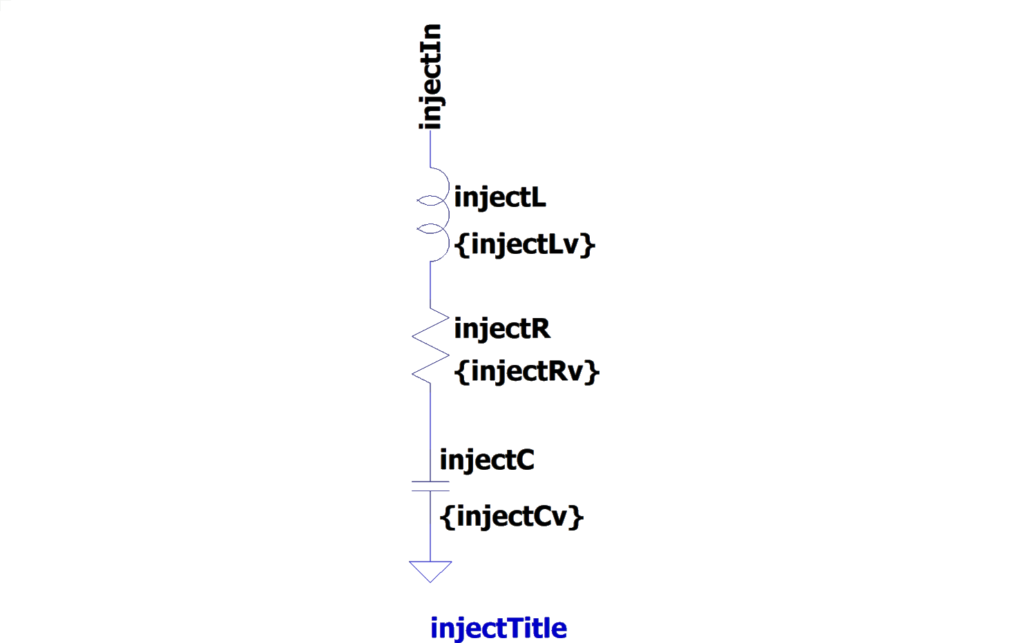
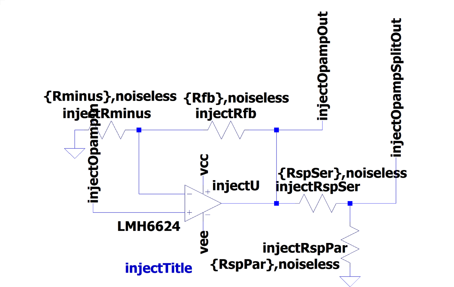
Figure 2: Blueprint templates for LTspice circuit.
The optimization script is coded in R language, and it can load these building blocks, assign values to the terminals to cross connect them to build the full circuit. Once the circuit is built, a Python subroutine is initiated to run the circuit in LTspice, and the resulting data is collected with Python code and analyzed. An outline of the optimization process is shown in Fig. 3.
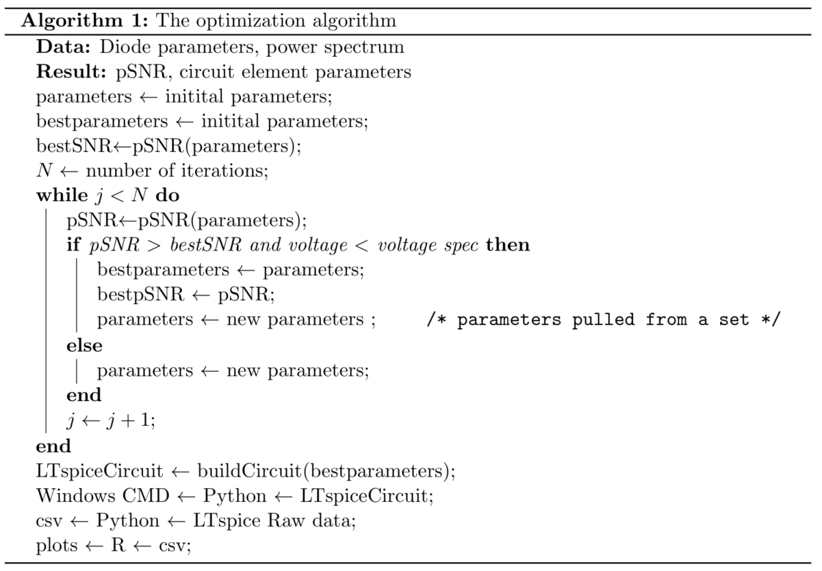
Figure 3: The flowchart for the algorithm.
The results
The optimization routine is a brute force search at the moment, however it will work well with smarter techniques such as simulated annealing. Also note that although the LTspice run is pushed to the end to simulate the final configuration, it can be pulled into the loop if there is a more complicated circuit to analyze. This might be a good tool for later projects. The optimization returns the best parameters, which are tabulated and compared to the values in the current circuit in Tab. 2.
| L7 | C30 | L9 | C35+C38 | L3 | C12+C15 | L1 | C2+C4 | L2 | C7+C10 | L4 | C16+C17 | L5 | C25+C26 | |
|---|---|---|---|---|---|---|---|---|---|---|---|---|---|---|
| V5 | 220nH | 100nH | 1.8 \(\mu\)F | 173.7pF | 390nH | 32.2pF | 390nH | 208pF | 180nH | 109pF | 100nH | 87pF | 100nH | 31pF |
| ReOpt | 4.0\(\mu\)H | 1\(\mu\)F | 2.9\(\mu\)H | 1.0\(\mu\)F | 0.9\(\mu\)H | 13.7pF | 9.4\(\mu\)H | 8.15pF | 0.35\(\mu\)H | 54.4pF | 1.7\(\mu\)H | 5.1pF | 2.9\(\mu\)H | 1.06pF |
We can compute the results for the optimized circuit as well as simulating it in LTspice. The results are shown in 4.
Figure 4: Optimized noise for the readout ports DC, 9.1MHz, and 45.5MHz. The solid lines show the calculated values and the dashed lines are from LTspice simulation. The critical values are marked on the plot.
We can now put together the results from the baseline circuit (V5) and the optimized circuit. The last line shows the gains.
| Circuit | DC | 9.1MHz | 45.5MHz |
|---|---|---|---|
| V5 | 11.0 mA | 1.000 mA | 1.690 mA |
| opt | 11.0 mA | 0.037 mA | 0.444 mA |
| ratio | 1.0 | 27.1 | 3.8 |
Figure 5 and Tab. 4 show the transimpedance for the 9.1MHz and 45.5MHz readout ports.
Figure 5: Transimpedance at the 9.1MHz and 45.5MHz ports.
| port / frequency | 9.1MHz | 45.5MHz | 18.2MHz | 36.4MHz | 54.6MHz | 91MHz |
|---|---|---|---|---|---|---|
| 9.1MHz | 1340.2 | 45.3 | 5.6 | 1.1 | 5.4 | 3.5 |
| 45.5MHz | 56.0 | 317.6 | 1.1 | 2.6 | 12.0 | 3.9 |
Note that in our model, the cross terms do not degrade the SNR as long as they are kept below a threshold so that they don’t saturate the OPAMP, see Eqs. (6)-(8). As the mixed signal passes through the OPAMP, it is amplified by a factor of 10, and feeds into the mixer, which will remove the cross terms, see the post LIGO modulation.
In Figs. 6,7, and 8, we show the noise spectrum for the DC, 9.1MHz, and 45.5MHz readout for the current circuit(V5) and the optimized circuit.
Figure 6: Comparison of the noise spectrum in its current equvalent at the DC output. The critical values are marked on the plot.
Figure 7: Comparison of the noise spectrum in its current equvalent at the 9.1MHz output. The critical values are marked on the plot.
Figure 8: Comparison of the noise spectrum in its current equvalent at the 45.5MHz output. The critical values are marked on the plot.
Finally, in Figs. 9, we show the break out of the squared noise for 9.1MHz and 45.5MHz outputs.
Figure 9: Break out of the squared noise at 9.1MHz and 45.5MHz outputs.
Parting words
Although I have no affiliation with LIGO, I know a few people who work/worked there. This optimization problem was thrown at me as a challenge by an engineer who used to work at LIGO. I shared my findings with a few people from the organization and I am hoping that they will take a closer look and see if this is worth pursuing. Meanwhile, since all the information I used here was public already, I decided to put parts of my analysis in my blog in case someone on the internet finds it entertaining. If someone else at LIGO finds this useful, that will be even better! Contact me if you have questions!